Etching with low-pressure plasma
High-precision surface etching
Flexible application-optimized process
Virtually all sorts of organic material can be plasma etched. The etching effect is based on the same chemical reactions as the cleaning effect. Only the parameters such as time and intensity must be adjusted to the requirements.
In addition to oxygen, other gases can be used which increase the etching rate significantly. In most cases, fluorinated gases as CF4 are employed. The fluorinated radicals created in these processes are much more reactive than oxygen plasma. Their reaction products, however, must be retained by suitable filters.

Advantages of plasma etching
- High crack penetration, therefore also suitable for micro holes
- Virtually all dielectrics etchable
- No toxic chemicals necessary
- Simultaneous treatment of all holes
- Low operating costs

Ecological and economical benefits
Compared with conventional wet-chemical methods, plasma treatment uses very little chemicals and the mainly used process gases (e.g. oxygen, nitrogen or CF4) are harmless, easily available and inexpensive.
Therefore there are no significant expenses for occupational safety or waste disposal. Energy consumption is relatively low and there is no need of a drying process of the components because it is a dry-chemical process.
Desmearing / Back-etching
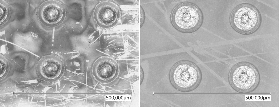
One application in plasma technology is desmearing or back-etching of mechanically drilled circuit boards. This process can be applied simultaneously to both sides of the board and all holes. Due to the outstanding crack penetration of the plasma process, holes of < 0.3 mm can be back-etched, even materials such as Teflon.
Modern circuit boards

Modern circuit boards and many other electronic components base on high-grade films
Processing can take place both by plasma etching and plasma activation

Areas of application
- Semiconductor industry
- Circuit board industry
- Microelectronics
- MEMs
Example
Photoresist stripping
During the manufacture of microelectronic devices, removal of photoresist layers very often is an inevitable process step. By isotropic strip processes with plasma, such removal of organic layers is possible without any plasma damage. As an experienced provider of low-pressure plasma systems for surface treatment, PINK also offers customized plasma systems for resist removal.
Read more: Photoresist stripping, PDF 87 KB More examples


